
The main objectives of this WP are to demonstrate the interest of optically biased chalcogenide glasses to design reconfigurable microwave devices. It is of course in direct link with the development of the chalcogenide glasses deposition process made in WP1. It will also prepare, together with WP3, the final multireconfiguration demonstrators developed in WP4.
The 3 main tasks initially identified in this WP are the following:
- Development of simple reconfigurable circuits based on chalcogenide glasses
- Study and development of optical biasing architectures
- Design and measurements of optically reconfigurable filters and antennas
A quick description of the work progress in each task is presented below.
Development of simple reconfigurable circuits based on chalcogenide glasses
The design and fabrication of such simple and well-known circuits aims at present the first proof-of-concepts and mainly complete, in-situ, the microwave characterization of the chalcogenide materials (permittivity in amorphous state, conductivity in crystalline one, losses, etc.). This characterization will be made using a retro-simulation process based on the measured responses of these simple circuits.
At that time, most of the circuits are ready (see some examples in Figure 2.1) and we only wait for the finalization of the deposition process (WP1). A first circuits fabrication run is planned for April 2022.
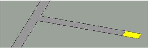
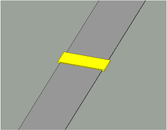
Figure 2.1 – Examples of simple reconfigurable circuits (shunt stub and series switch) for chalcogenide materials characterization.
Study and development of optical biasing architectures
In the first task of this WP, we will use heating process first to switch the chalcogenide materials from amorphous to crystalline states. We will also quickly use non-integrated laser source for photo-induced optical control. Several lasers have been identified and are available from our partner FOTON Institute, recently integrated in DATERAC project. All the available lasers will allow us to test different configurations in Continuous Wave (CW) with different wavelengths (405 nm, 532 nm and 1064 nm) or in pulsed mode (Laser TI or OPO).
In order to develop the manufacturing process between our partners, ISCR and FOTON, chalcogenide glasses deposition are currently in progress on 2 substrates. The first one is consist of a full plate deposit of chalcogenide glasses without any further step. It will mainly used for materials chalcogenide characterizations (see WP1). The second one will consists of some glasses areas closed in shape and size to the structures used in the demonstrators developed in the third task of this WP. A lift-off process will be used here. The layout of this second substrate is presented in Figure 2.2.
Figure 2.2 – Layout of the second substrate (blue areas represent chalcogenide glasses depositions after lift-off process).
The goal of this substrate is to determine the best switching configuration between amorphous and crystalline states. Several tests are so considered to determine the best compromise between wavelength, power density, illumination time, pattern shape, etc.
Note that the teams of FOTON Institute and IETR Lab involved in this project are in the same place (Campus INSA Rennes). This proximity is very important for us because it will greatly simplify the access to this facilities and reduce characterization time.
Design and measurements of optically reconfigurable filters and antennas
We firstly focus on reconfigurable filter and more especially on DBR filter, well-known by the team [1-4]. DBR filters can easily be reconfigured in terms of central frequency and bandwidth independently and simultaneously by controlling the electrical length of all the stubs that constitute it. Nevertheless, the use of an electrical control of reconfigurable elements such as PIN diodes, varactors or MEMS, implies the introduction of biasing lines (one per element) that could quickly complicate the whole circuit design due to the need to isolate the DC part to the RF ones.
In the DATERAC project, we propose to use an optical control to modify the length of the stubs. Chalcogenide materials are added at the end of each stub. In their amorphous state, this material presents a high resistivity and is more or less transparent to the wave propagation. The circuit is so centered around an initial frequency (F1) and presents an initial bandwidth (BW1). When we change the state of the chalcogenide glasses to their crystalline state at the stub extremity, the pieces of materials now present a low resistivity and so act as transmission lines. The center frequency then decreases to a second one (F2) and the bandwidth could be modified to a new value (BW2). Nevertheless, if the frequency shift is relatively important, the matching level in the pass band is severely degraded. We so propose a way to compensate for this degradation adding other chalcogenide glasses areas wisely in the circuit.
The proposed concepts not being published yet, they are not more detailed here for the moment.
[1] C. Quendo, E. Rius, C. Person, “Narrow bandpass filters using Dual-Behavior Resonators”, IEEE Transaction on Microwave Theory and Techniques, vol. 51, n°3, pp 734-743, March 2003.
[2] E. Fourn, C. Quendo, et al., “Bandwidth and central frequency control on tunable bandpass filter by using MEMS cantilevers,” in IEEE MTT-S Microwave Symposium Digest, vol. 1, pp. 523-526, Philadelphia, PA, USA, Jun. 2003.
[3] C. Quendo, et al., “General synthesis of N-band resonator based on N-order dual behavior resonator”, IEEE Microwave and Wireless Components Letters, vol. 17, n°5, pp. 337-339, May 2007.
[4] E. Fourn, C. Quendo, E. Rius, “Novel n-band tunable resonator based on n-order Dual-Behavior Resonator and tunable capacitors,” International Journal of Microwave and Wireless Technologies, vol. 8, no. 1, pp. 15-23, Feb. 2016.