
Fig. 1 shows the block diagram of the first architecture explored: photonic beam switching. First, the optical tones modulated according to a data string are carried by an optical fiber. Then, the optical input is directed to one of the \( N \) elements by an optical switch. Next, the light illuminates a photdiode (PD) connected to the antenna that will radiate the modulated mm-wave carrier. For beam switching, the antennas are located at the back focal plane of a lens with focal length \( f \), as shown in Fig. 1. When the antenna is placed at a distance \( s \) out of the optical axis, the beam tilt is given from geometrical optics by \( \tan \theta = \pm s/f \), where \( \theta \) is the angle measured with respect to broadside, and the sign depends on the clockwise direction of \( \theta \). Only one element is active at a time, and the beam can be switched among \( N \) different directions given by (1). In general, lens systems present field of views narrower than phased arrays, but the proposed architecture fully serves for beam alignment purposes in point-to-point links.
The beam switching technique applied to a photonic-enabled mm-wave transmitter presents several trade-offs that make it a very interesting route to explore. First, it is possible to achieve a high directivity due to the lens, which does not depends on the number of elements, \( N \). In principle, \( N \) can be low, and given the cost of III-V components, it is desirable to use as few as possible to fulfill the system requirements. In practice, this will depend on the desired field of view of the transmitter, so the technique is very well suited to applications where only a few beam directions are required, e.g., to compensate misalignment between the emitter and the receiver in point-to-point links.
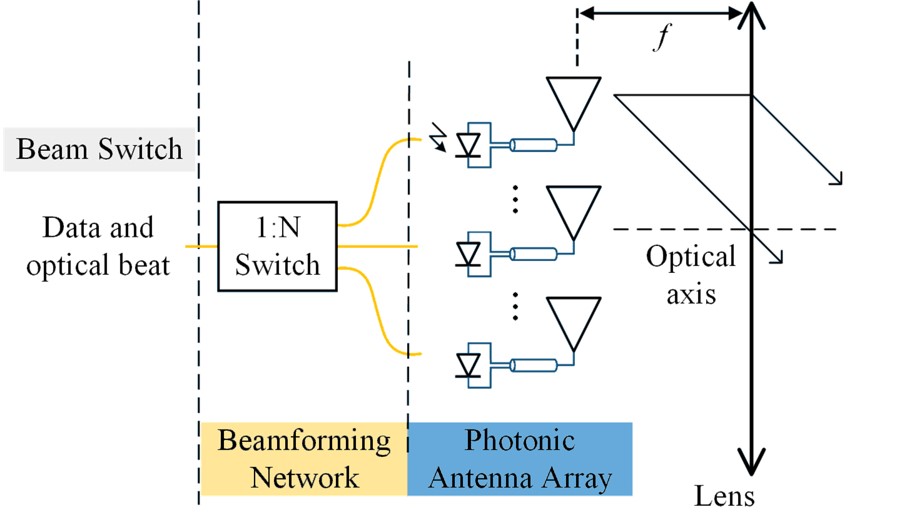
Fig. 1: Architecture of a mm-wave antenna array excited photonically for beam switching.
Fig. 2 shows the assembly of the antenna array used as primary feed of a dielectric lens. For validation, we also show measurements of the radiation pattern and return loss of a prototype excited with a ground-signal-ground (GSG) probe. The array has been fabricated using printed circuit board (PCB) technology on a 127 \( \mu\)m-thick, high-frequency Duroid 5880 laminate (\( \epsilon_r\) = 2.24, tan\( \delta\) = 0.004 at 60 GHz).
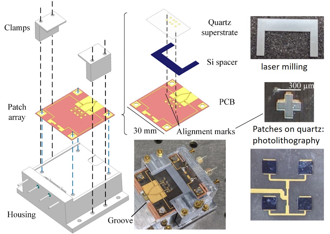
Fig. 3a shows the measured and simulated values of the reflection coefficient of the structure shown in Fig. 2. The continuous black line refers to the measurement when the probe is de-embedded. The measured reflection coefficient shows a good agreement with the simulated values in the frequency range that can be tested with the available W-band mm-wave extension head and probe. Discrepancies between simulated and de-embedded curves are attributed to an inaccurate determination of PCB substrate parameters: \( \epsilon_r\) and thickness, as well as to tolerances in the PCB manufacturing process. To illustrate this, the dashed grey line of Fig. 3a shows the simulated results for a deviation in \( \epsilon_r\) of 0.04 from the nominal value (\( \epsilon_r=2.28\)). This deviation could in part explain the horizontal shift between the simulated and the measured curves for the highest values of \( \S_{11}\) near 84 GHz.
Fig. 3c shows the measured and simulated normalized directivity at 80 GHz. The relatively high side-lobe at -50° occurs due to radiation leakage from the S-bend of the 50 \( \Omega \) microstrip line that feeds the sub-array. The side-lobe level stays below -10 dB up to 83 GHz. In the measurements, the ripples in the curves are due to the interference coming from the probe tip. The measured cross-polarization levels are < -15 dB at broadside. It is also possible to obtain the antenna gain, and the measured and simulated results are shown in Fig. 3b. A maximum deviation of 0.8 dB with respect to full-wave simulations is obtained, with measured gain values of 12.3 \( \pm 0.7\) dB between 75-87 GHz. The estimated radiation efficiency is > 75 % at E-band frequencies.
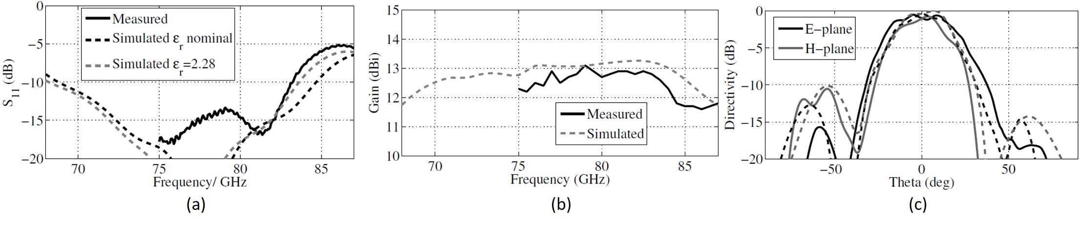
Fig. 3: (a) Magnitude of the reflection coefficient of the prototype. Dashed line: simulated values, continuous line: measured after de-embedding. (b) Simulated and measured gain of the prototype. (c) Normalized directivity at the E- and H-planes for 80 GHz. Continuous line: measured values, and dashed line: simulated values.
To realize photonic beam switching, the antenna array is placed at the focal plane of a PTFE lens (Thorlabs LAT075) with a back focal length (bfl) of 53 mm and a diameter of 5 cm (Fig. 4a). The two sub-arrays lie symmetrically s = 2.5mm above and below the optical axis. Excitation of one of either photodiodes produces a tilted beam at an angle 2.7 degrees, which would assist in fine beam alignment. The simulation results of the antenna plus lens using ANSYS HFSS’ Finite Element-Boundary Integral (FE-BI) boundary conditions are shown in Fig. 4b for 75 GHz and in Fig. 4c for 85 GHz. The figures also show the measured values. The half-power beamwidths are 5.2° and 4.8°, respectively, and the simulated directivities are 27.5 dBi and 27.9 dBi, respectively. For a separation between sub-arrays of 5mm, the beam crossover occurs approximately at -3 dB, as can be observed in Fig. 3. Furthermore, the pointing direction is stable within +/-0.1° across the E-band.
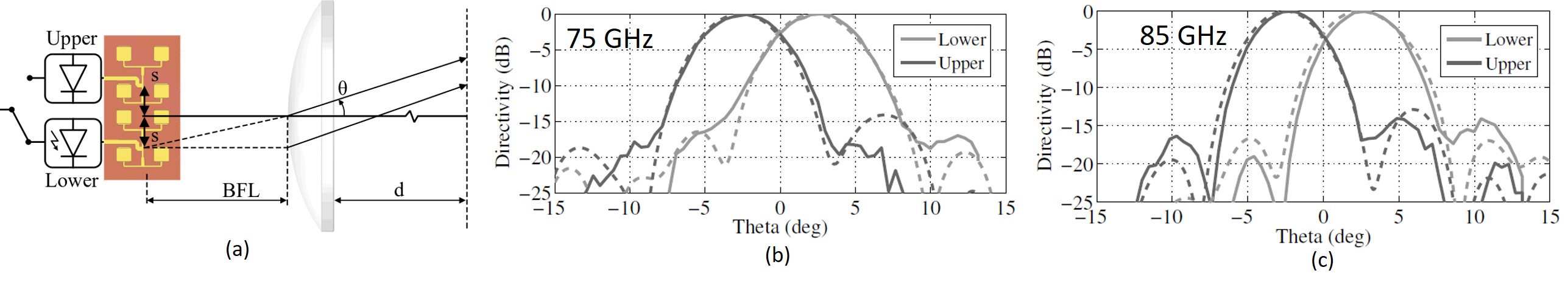
Fig. 4 (a) Measurement set-up. (b)-(c) Measured (continuous line) and simulated (dashed line) normalized radiation patterns versus elevation angle for the experimental characterization of photonic beam switching for (b) 75 GHz, and (c) 85 GHz. Lower and Upper refer to the sub-array position respect to the optical axis.