
UMR CNRS 6082 – FOTON – Fonctions Optiques pour les Technologies de l’informatiON
INRIA Rennes – Bretagne Atlantique – IRISA UMR CNRS 6074
UMR CNRS 5270 – Institut des Nanotechnologies de Lyon – Ecole Centrale de Lyon
Abstract: 3D integration in the ultra deep submicron domain means the implementation of billions of transistors or of hundreds of cores on a single chip with the need to ensure a large number of exchanges between cores, and the obligation to limit the power consumption. Focusing on system integration rather than transistor density, allows for both functional and technological diversification in integrated systems. The functional diversification allows for non-digital functionalities to migrate from the board level into the (on-)chip level. This allows for integration of new technologies that enable high performance, low power, high reliability, low cost, and high design productivity. Use of Optical Network-on-Chip (ONoC) promises to deliver significantly increased bandwidth, increased immunity to electromagnetic noise, decreased latency, and decreased power consumption while wavelength routing and Wavelength Division Multiplexing (WDM) contributes to the valuable properties of optical interconnect by permitting low contention or even contention free routing. WDM allows for multiple signals to be transmitted simultaneously, facilitating higher throughput. Individual realization of CMOS compatible optical components, such as, waveguides, modulators, and detectors lets the community foresee that such integration may be possible in the next ten years. The aim of the project is therefore to investigate new optical interconnect solutions to enhance by 2 to 3 magnitude orders energy efficiency and data rate of on-chip interconnect in the context of a many-core architecture targeting both embedded and high-performance computing. Moreover, we envisage taking advantage of 3D technologies for designing a specific photonic layer suitable for a flexible and energy efficient high-speed optical network on chip (ONoC).
This project proposes to investigate how the introduction of novel optical technologies could improve the energy efficiency and enhance the data rate of interconnects used in many-core architectures for embedded and high-performance computing. In particular, it will design and optimise flexible and energy efficient high-speed optical networks on chip (ONoC) making use of 3D technologies. These goals will be achieved thanks to 3D architecture studies combining electrical and optical interconnects. Novel devices, and in particular light sources and nonlinear elements suitable for those applications that can be monolithically integrated on the silicon platform will be investigated and fabricated. High- and low-abstraction models for the simulations of optical links and complete ONoCs making use of such devices will be implemented. Finally, the potential of novel all-optical signal processing functionalities exploiting micro- and nano-optical devices will be evaluated in the context of the previously defined architectures where those may be used.
The originality of the proposed approach is that it combines the expertises of leading research groups focusing on energy-efficient computer architectures and reconfigurable systems on-chip, optical interconnects, novel optical devices based on the integration of semiconductor materials on the silicon platform, optical communications, and all-optical nonlinear signal processing. While many independent studies have been conducted individually on all those aspects, the consortium presents an added value by gathering all those expertises and consolidating interactions between the different actors and research communities in the fields of interconnects and optical networks on chip.
Scientific challenge
Defining new architectures while taking advantage of optical interconnects represents today a key issue for future 3D multi-processor system-on-chip (MPSoC) designers. This paradigm shift requires new methodologies that have to take into account the new constraints specific to optical interconnects. For instance, no clear solutions are available for integrating optical sources when considering cost and integration. The number of lasers will anyway be limited due to power-consumption and space occupancy.
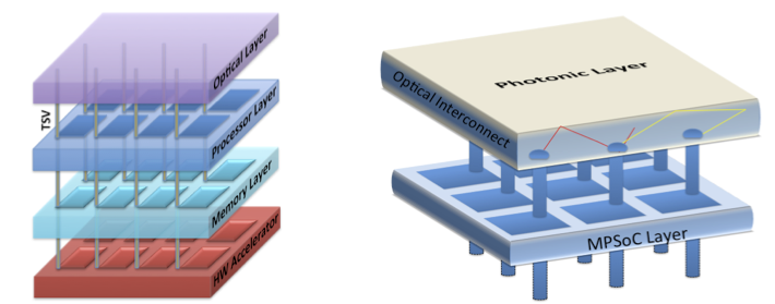
Figure 1: A 3D stacked many-core architecture and the detail of the multi-processor layer stacked with a dedicated optical interconnect layer
The aim of the project is therefore to investigate new optical interconnect solutions to enhance by 2 to 3 orders of magnitude the energy efficiency and data rate of on-chip interconnects in the context of a many-core architecture targeting both embedded and high-performance computing. Moreover, we envisage taking advantage of 3D technologies for designing a specific photonic layer suitable for a flexible and energy efficient high-speed optical network on chip (ONoC). The left-hand side of Figure 1 shows a 3D-stacked many-core architecture, where several layers of functional resources are stacked together and vertically connected by through silicon vias (TSVs). On the right part of the figure, the detail of a potential multi-processor layer stacked with a dedicated optical interconnect layer is presented.
To reach this goal, we propose to take advantage of 3D stacking technologies to build a new kind of optical interconnect layer. From the generic architecture of a multi-processor layer stacked with a dedicated optical interconnect layer, as represented in Figure 1, the work is distributed into four main challenges:
- The first challenge “Design space exploration of 3D architectures using ONoC” is to explore the design space of 3D architectures using optical networks on chip (ONoC). The main constraints will be to have a global interconnect with high flexibility, energy efficiency, and operating at high-speed. We will study how to partition functionalities between electrical and optical interconnects, how many vertical links should be used and if digital encoding/decoding of data to route in the ONoC (e.g. code division multiple access, CDMA) is required to improve performance. The main partners in this challenge will be INRIA and INL, but with a strong feedback from photonics specialists from FOTON-Photonics Systems.
- The second challenge “Novel laser sources monolithically integrated on silicon” is the search for new photonic devices, including a laser source monolithically integrated on silicon. More specifically, the use of the GaP-on-Si platform to build edge-emitting lasers and micro-disk photonic devices will be studied. The main investigator is FOTON-OHM with the help of INL on layout, power and performances constraints due to ONoC design.
- The third challenge “Models of photonics devices and global simulation of the computing architecture” is to develop functionalities and components models and simulation setups of the global computing manycore architecture. Heterogeneous and hybrid (optical, analog, and digital) simulation models are required here for accurate performance evaluations and will be defined according to the new photonic devices developed at FOTON-OHM. Partners of this challenge will be INRIA and INL. This challenge will be based on results produced in Challenge 2 for device models and in Challenge 4 for new functionality proposals, and will serve as a basis for Challenge 1.
- The last challenge “New optical functionalities for on-chip transmission and signal processing” deals with modeling and proof-of-concept demonstrations of new optical functions in order to assess the potential and efficiency of various components and technological approaches. In particular, we will investigate how to take advantage of the wavelength and spatial degrees of freedom that are inherent to optics to perform on-chip all-optical signal processing functionalities. Feasibility studies will be performed, resulting in consolidated inputs to the architecture studies. The work will essentially involve FOTON-Photonic Systems, with strong interactions with INRIA and INL.
Team
The 3DCore team is composed of academic staff of University of Rennes 1, INRIA, CNRS, Ecole Centrale de Lyon and INSA engineering scools membres of three labs located in Brittany and in Lyon IRISA (Lannion, Rennes), FOTON (Lannion, Rennes) and INL (Lyon).
FOTON: Pascal Besnard, Christophe Peucheret, Patrice Féron, Yoan Léger, Olivier Durand, Alberto Parini, Yannick Dumeige, Yann Boucher, Ronan Tremblay, Charles Cornet
IRISA/INRIA: Daniel Chillet, Olivier Sentieys, Cédric Killian, Jiating Luo (PhD), Martha Johanna Sepulveda Florez (PostDoc until Sept. 2015), Van-Dung Pham (PhD), Ashraf El-Antably (PostDoc since April 2016)
INL: Sébastien Le Beux, Ian O’Connor, Xavier Letartre, Christelle Monat