
3D Many-Core Architectures based on Optical Network on Chip
UMR CNRS 6082 – Institut FOTON – Fonctions Optiques pour les Technologies de l’informatiON
INRIA Rennes – Bretagne Atlantique – IRISA UMR CNRS 6074
UMR CNRS 5270 – Institut des Nanotechnologies de Lyon – Ecole Centrale de Lyon
Abstract
This project proposed to investigate how the introduction of novel optical technologies could improve the energy efficiency and enhance the data rate of interconnects used in many-core architectures for embedded and high-performance computing. We explored the design of 3D architectures of these hybrid photonic-electronic microprocessors at several scales: from the system architecture and circuit levels, to the physical level of photonic circuitry and individual photonic components such as integrated lasers. We proposed and optimised flexible and energy efficient high-speed optical networks on chip (ONoC) making use of 3D technologies. Novel devices, such as light sources, nonlinear functions, or routing components suitable for those applications, were investigated and active photonic resonators monolithically integrated on the silicon platform were fabricated. High- and low-abstraction models for the simulations of optical links and complete ONoCs making use of such devices were implemented. Finally, the potential of novel all-optical signal processing functionalities exploiting micro- and nano-optical devices were assessed in the context of the previously defined architectures.
The originality of the proposed approach was that it combined the expertise of leading research groups focusing on energy-efficient computer architectures and reconfigurable systems on-chip, optical interconnects, novel optical devices based on the integration of semiconductor materials on the silicon platform, optical communications, and all-optical nonlinear signal processing. While many independent studies had been conducted individually on all those aspects, the consortium presented an added value by gathering all those skills and consolidating interactions between the different actors and research communities in the fields of interconnects and optical networks on chip.
3DCORE has led to two ANR projects, ANR PRCE “Opticall2” and ANR JCJC “SHNOC”, which can refer to results and contributions obtained within this project.
The pdf version of the final report can be downloaded here.
1.Project Overview
1.1 Initial goals
Defining new architectures while taking advantage of optical interconnects represents today a key issue for future 3D multi-processor system-on-chip (MPSoC) designers. This paradigm shift requires new methodologies accounting for the new constraints specific to optical interconnects such as multiplexing issues, laser scalability or thermal management. The aim of the project was therefore to investigate new optical solutions to enhance the energy efficiency and data rate of on-chip interconnects in the context of new many-core architectures, and to explore the design space offered by this new paradigm using simulations. We focussed on a 3D MPSoC architecture (Fig. WP1-(a)) where a photonic layer featuring an Optical network on chip (ONoC) is used to interconnect several heterogenous execution resources implemented onto specific microelectronic layers. The goal of the project was not to design and fabricate such a 3D microprocessor prototype, but i) to propose and analyze new disruptive ideas for optical interconnects, ii) to design and characterize new devices, as well as iii) to demonstrate a virtual prototype of the global architecture, mainly using simulations.
1.2 Project organization
In order to explore the design of a 3D hybrid many-core architecture including an optical interconnect layer, the project was distributed among four main challenges:
- The first challenge was dedicated to design space exploration of 3D architectures using optical networks on chip (ONoC). In order to account for issues of flexibility, energy efficiency and high-speed operation, the partition of functionalities between electrical and optical sub-systems has been investigated. We proposed specific communication protocols and on-line adaptative configuration management rules depending on the processor instantaneous needs. The main partners in this challenge were INRIA and INL, but with a strong feedback from photonics specialists from Institute FOTON-Photonics Systems.
- The second challenge consisted in the exploration of integrated laser on silicon architectures for efficient on-chip optical routing. We investigated state-of-the-art designs and assessed their relevance depending on the many-core architecture requirements. From this, we developed laser models suited for their integration into higher level simulations of challenge 3. We also worked on the implementation of a monotlithic III-V/Si integration platform for the realisation of active and nonlinear photonic devices on chip in connection with Challenge 4. The main investigator was Institute FOTON-OHM.
- The third challenge was to develop functionalities and components models and simulation setups of the global computing many-core architecture, based on results produced in Challenge 2 for device models and in Challenge 4 for new functionality proposals. This challenge was also an input for Challenge 1. Several ONoCs architectures were investigated. Data routing reliability was optimized through the reduction of cross-talk into the optical network. Adaptative ONoC solutions in term of energy consumption and data rate were proposed for integration into the flexible architectures developed in Challenge 1. Partners of this challenge were INRIA and INL.
- The last challenge dealt with modeling and proof-of-concept demonstrations of new optical functions in order to assess the potential and efficiency of various components and technological approaches. In particular, we investigated both the issues raised by wavelength division multiplexing and mode division multiplexing when applied to photonic integrated circuit components. We also explored nonlinear switching functionalities in connection with Challenge 2. The work essentially involved Institute FOTON-Photonic Systems, with strong interactions with INRIA and INL.
2.Scientific Results
In this section, the descriptions of the project results are presented for each of the four project challenges cited above.
2.1 Challenge 1: Design Space Exploration of 3D Architectures using ONoC
Designing multiprocessor architectures based on Optical Network on Chip is a challenging task when considering the tuning of all the different parameters to ensure high performance at application level.
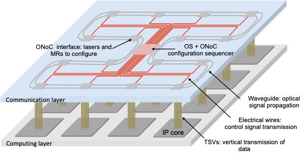
WP1 – (a) Proposed 3D ONoC with: an electrical layer with cores, an optical layer with photonic on silicon links, an Operating System and ONoC configuration sequencer to distribute communication strategies.
In particular, one of the major problems is to propose a network interface that can exploit opportunities offered by the optical medium. Moreover, it is important to expose an Application Programmer Interface (API) at operating system level that offers the possibility to manage the optical network. In this context, the challenge consists in exploring different possible ONoC configurations and to define the one available at run time. Challenge 1 addressed the following topics, as summarized in Fig. WP1-(b):
- Definition of the communication model for Optical Network on Chip. In this topic, we extracted a high-level performance model of optical communications including losses induced by all optical components. All the different losses that can appear during the communications were modeled. This model helped us to propose a high-level management strategy.
- Definition of an interface to connect electrical and optical domains. We defined all the functionalities needed to ensure communication from source to destination and we also defined hardware blocks to manage these communications. Serialization, deserialization and wavelength allocator blocks have been developed with very strict timing constraints to ensure high-speed link with the optical components. We also proposed hardware blocks to manage the laser power, which is the most critical part when considering power consumption of the optical communication.
- Definition of the strategies (communication protocol) to manage the communication medium. This topic concerned the definition of high-level mechanisms, which can handle the allocation of the communication medium for each data transferred between tasks. This consists in defining the protocol for wavelength allocation, in particular in the context of wavelength division multiplexing. This protocol produces a set of communication configurations, which are defined by the number of wavelengths, a set of wavelengths for each communication, the level of quality for the communications, and the laser powers used. We also introduce Error Correcting Codes (ECC) in the communication channel to ensure link reliability. Due to the number of parameters of these configurations, we use a multi-criteria optimization technique to produce them.
- Definition of new high-level techniques to manage the configurations on-line. The objective of this part consisted in providing all the information to the operating system to be able to decide which configurations must be applied for a given communication at a specific time. To this aim, we developed a sequencer able to exploit on-line the set of configurations to respect the application constraints.
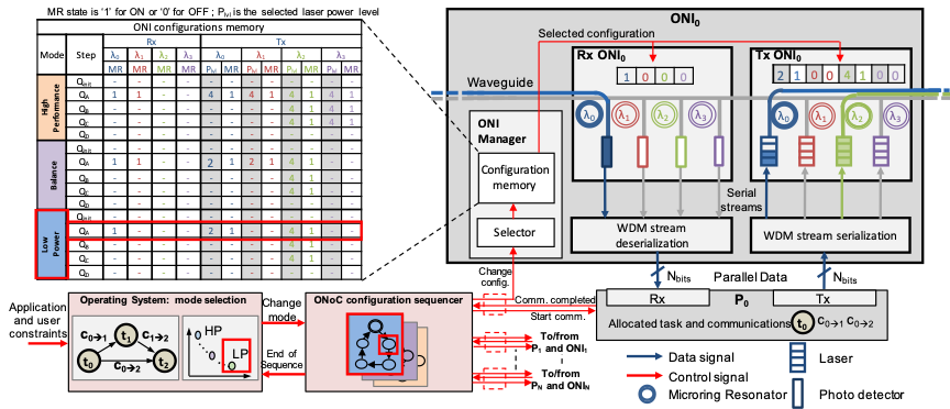
WP1 – (b) Proposed Optical Network Interface (ONI) and application of the communication configuration optimized from Challenge 3. The proposed approach requires two hardware blocks: an ONI manager, located in each ONI, in charge of activating the Lasers and MR, and an ONoC configuration sequencer, that is shared among all the ONIs, in charge of sequencing the configurations of the ONIs. An Optical Network Interface, ONI (right part), integrates a receiver Rx and a transmitter Tx. The transmitter is composed of on-chip laser sources that each on them can emit and inject optical signal at a specific wavelength into the waveguide. The power generated by the Lasers can be configured. In this example the Lasers can be configured independently among four levels of power. The data are directly transmitted from these lasers through current modulation (OOK) and each laser source can also be turned OFF for energy saving. As the lasers are sending data in serial and as a core sends data in parallel on Nbits, a WDM stream serialization is required in order to perform the serialization and the allocation of the serial data onto the selected wavelengths (i.e. lasers). The receiver part includes wavelength-specific MR that can be turned ON or OFF to configure respectively drop or pass-through operations of the signals at a given wavelength. Signal dropped from a waveguide reaches a photodetector, where opto-electric data conversion generates an electrical signal suitable for the electronics part of the receiver. The considered architecture allows the reuse of wavelengths to realize multiple independent communications in a single waveguide. The receiver includes a WDM stream deserialization to perform serial to parallel conversion on the received data. Each ONI includes an ONI Manager in charge of configuring the receiver and the transmitter. It includes an ONI configurations memory which stores the configurations to apply on the MR and Lasers for different operating modes and at different steps composing a sequence of configurations. The second hardware block required is the ONoC configuration sequencer in charge of synchronizing all the ONI Managers of the ONoC. It includes a state machine expressed as a sequence diagram. This block takes as input decision from the Operating System in order to select the configuration mode satisfying application requirements. Moreover, it is connected to the ONIs through three signals. The first is a one-bit signal indicating the ONI to start exploiting the configuration associated to the current Step and Mode selected in the ONI configuration memory. The second is also a one-bit signal generated by the ONIs indicating that a step is over. The last signal bit-width depends on the number of Modes embedded in the ONI configuration memory and allows to select the mode to apply.
2.2 Challenge 2: III-V laser on silicon
The goal of this challenge was twofold: i) providing the expertise in the physics of laser on-chip integration to ensure the sustainability of the architectures simulated; ii) Developing a gallium-phosphide (GaP) based laser monolithically integrated on silicon (Si).
For the first goal, we built a cartography of lasers suited to on-chip integration, from an exhaustive review of the state of the art. The lasers were classified according to criteria suited to the specifications of on-chip optical interconnects (Fig. WP2-(a)). This study reveals that laser integration is still a vivid challenge with lasers hardly matching the criteria for practical integration, even if eligible candidates start emerging. Based on this study, we developed a numerical model of integrated laser performances for photonic routing simulations, taking into account the scalability of laser performances (efficiency, output power, modulation speed) vs. the laser dimensions.

Fig. WP2-(a) Left panel: Performances of state-of-the-art lasers either integrated or easily integrable on Si. The green region shows the features required for practical ONoC integration. Right panel: Scalability law of state-of-the-art integrated lasers output power, which goes beyond the laser architecture itself.
The inclusion of this model into the architectures developed in challenges 1 and 3 is in progress. We also modeled thermal management in lasers integrated on silicon with two opposite approaches: i) the heterogeneous integration, based on the bonding of III-V laser structures or gain area onto Si photonic integrated circuits; ii) the monolithic approach where the III-V materials are directly grown on the Si substrate. Our results show that the monolithic approach, despite the defects created at the interface between III-V and Si could be an interesting way to ensure thermal dissipation of the laser induced heat. Conversely, the monolithic approach makes the lasers more impacted by fast temperature changes within the chip than heterogeneously integrated, which are mostly insulated from the Si part of the chip. The choice of laser platform thus greatly depends on the overall hybrid microprocessor design.
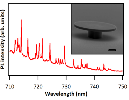
WP2-(b): Emission of the resonant modes of an active microdisk optical resonator based on GaP on silicon. The realization of high-quality-factor microresonators containing radiative emitters (such as quantum dots) is a first step for the realization of on-chip lasers for ONoCs. Inset: scanning electron microscope image of the device (scale bar : 1µm)
For the second goal, we could demonstrate the realization of photonic devices at the state of the art based on monolithical GaP on Si, from integrated microdisk resonators on silicon (see Fig.WP2-(b)) to electroluminescent diodes on Si. In particular, a detailed investigation of electrical injection and photonic confinement in AlGaP compounds has been carried out. Despite our efforts, the promotion of a direct optical transition in GaP-based nanostructures could not be demonstrated, preventing us from observing a laser effect, but we already reported a transition of quantum dot emitters from type II to type I.
2.3 Challenge 3: Models of photonics devices and global simulation of the computing architecture
To demonstrate the performance of the proposed ONoC architecture composed of photonics and electronics layers, we defined a framework able to simulate the execution of applications on such architecture (Fig. WP3-(a)). This platform is based on the application modeled as a task graph and provides the evaluation of the wavelength allocation to ensure each communication between cores supporting the task execution. The application is defined through a direct acyclic graph, and the wavelength division multiplexing technique is explored to evaluate not only the communication latencies, but also the power consumed by all the communications. For this exploration, the execution of the application is simulated using the optical component models, and the power consumption is computed by taking the optical and the electrical parts into account. The losses for the propagation of the optical signals are evaluated. Based on the model of the photonics components and of the architecture (in particular the number of photonics components included in each optical network interface), we compute the global loss as a function of the communication configuration (distance from source to destination cores, number of waveguide bends, etc.).
The use of wavelength division multiplexing generates crosstalk between optical signals. Therefore, we modeled these effects and include this crosstalk loss in the global model. We also explored other communication strategies, such as including error-correcting code, choosing the best set of wavelengths for each communication, and managing the laser power.
Because this architectural exploration is based on several parameters, the framework developed is based on using a genetic algorithm where the chromosomes include the parameters to explore. The genetic algorithm produces a set of possible solutions, defining a Pareto front of solutions. These different solutions define the tradeoff between energy and power consumption. From the results produced with the simulation/exploration platform, we are able to store the different possible solutions into a memory, which is called Configuration Memory. This memory is then used on-line by the operating system to apply one specific configuration depending on the context. For example, for an application which needs high performance, the solutions using several wavelengths for each communication could be used, even if these solutions consume more power. In contrary, for an application which is not constraint by execution time, the operating system can choose solutions using just one wavelength for each communication to reduce the power consumption of the optical part.
To sum-up, this simulation platform is used to extract, off-line, the different configurations of the communication, which are used, on-line, by the operating system to exploit the communication media based on the execution context.
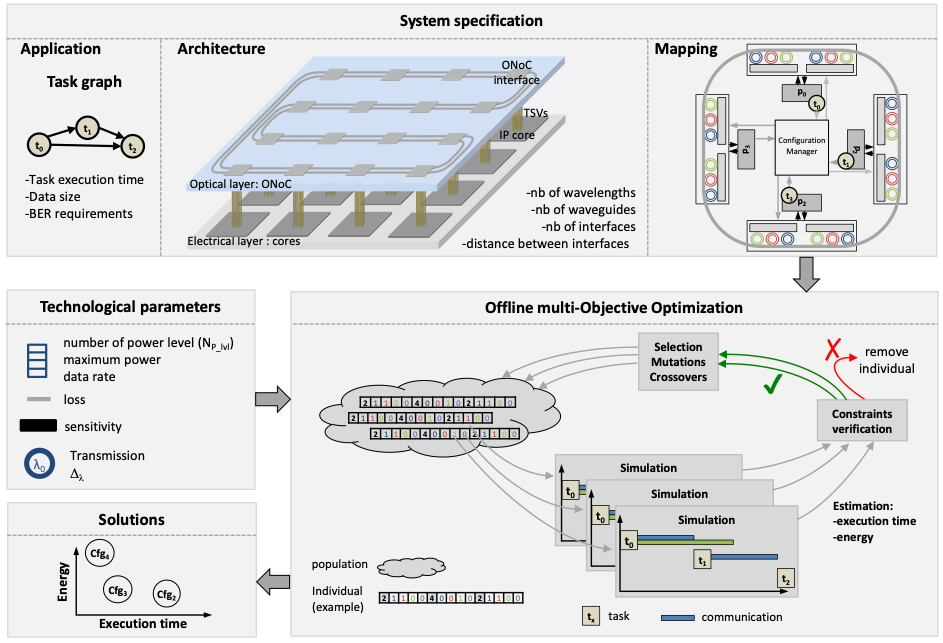
WP3 – (a) Description of the Framework developed to simulate the ONoC with user inputs and architectural parameters. The flow takes as inputs an application modeled as a task graph characterized by task execution times, amount of data transmitted between tasks, and minimum BER to be reached. The architecture includes an ONoC implemented on top of processing cores and characterized by a topology, a number of wavelengths and waveguides. The ONoC allows for cores to communicate with each other using optical signals, which is achieved using E/O and O/E conversion. The interfaces are crossed by waveguides propagating the optical signals using WDM in both clockwise and counter-clockwise directions which reduces the maximum communication distance. The mapping of the tasks on the cores gives the communications in the ONoC.
Based on a set of device and system input parameters, a multi-objective optimization is carried out using a genetic algorithm due to the two contradictory objectives. In our genetic algorithm, the ONoC configuration modes are represented by chromosomes and the genes encode both wavelength allocations and laser power levels. Then a simulation is carried out to estimate application execution time and total ONoC energy consumption (i.e. the algorithm fitness functions). Finally, the resulting ONoC configuration modes on a Pareto front from the multi-objective optimization are thus reported, including low-power solutions, which tend to minimize the number of used wavelengths, and high-performance solutions, for which multiple wavelengths are allocated to shorten the communication time.
2.4 Challenge 4: New optical functionalities for on-chip transmission and signal processing
This workpackage has been dedicated to exploratory studies of new optical functionalities potentially relevant for future optical networks on chip (ONoCs). In this context, the relevant functionalities deal with multiplexing, in order to meet the very high throughput requirements of such interconnects, and switching, in order to implement the necessary network reconfigurability and dynamic operation.
As far as multiplexing is concerned, we have explored traditional wavelength division multiplexing (WDM) as well as a novel approach based on mode division multiplexing (MDM) (Fig. WP4-(a)). The implementation of switching functionalities is dependent on the availability of suitable nonlinear materials that could be integrated on the silicon platform, either by bonding techniques or direct growth. This point is strongly connected to Challenge 2, where the relevant technological aspects have been addressed.
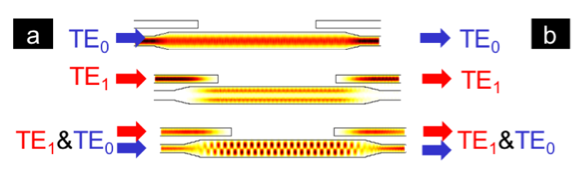
WP4 – (a) Illustration of the principle of on-chip mode-division multiplexing. (b) Layout of one of the investigated devices (mode router based on a micro-ring resonator) providing optical functionalities for mode multiplexing.
The following studies have been conducted, and the following main results have been obtained:
- A ring network architecture has been investigated in Challenges 1 and 3. We have evidenced a potentially deleterious effect of spurious resonances in the transfer functions of optical paths along this topology, and numerically investigated this effect.
- We have performed network dimensioning studies aiming at comparing the MDM and WDM approaches in terms of throughput, power budget, power consumption and footprint. The studies have to a large extent been so-far restricted to the case of point-to-point links.
- Various mode-multiplexing functional devices have been analyzed thanks to an analytic approach based on scattering parameters.
- Passive mode-manipulation devices, which would act as building blocks in future ONoCs employing MDM, have been investigated theoretically and numerically. These devices include mode (de)multiplexers, mode converters, multimode optical add-drop wavelength multiplexers, etc. When the density of interconnects increases, crossings between waveguides will become inevitable. We have also investigated such structures.
- Based on the previous numerical investigations, we have initiated a collaboration with the Guided Optics and Sensors Group at FOTON Institute in order to demonstrate selected multimode functionalities, including modal add-drop multiplexers, multimode micro-ring resonators and multimode crossings, on a polymer waveguide platform. A first generation of devices has been processed and characterized.
- Most demonstrations of on-chip MDM systems are, so-far, point-to-point links. The implementation of on-chip networks exploiting the modal dimension has not been reported yet. We have therefore engaged in an informal collaboration with the Department of Photonics Engineering at the Technical University of Denmark (Dr. Yunhong Ding) in order to design, fabricate, and perform system characterizations of an on-chip mode-multiplexed network based on a ring-network topology. Some first building blocks have been fabricated in Denmark on the silicon-on-insulator platform based on our designs, then tested at FOTON Institute.
- A numerical and experimental investigation of cross-talk in systems using either WDM or MDM has been conducted. For MDM systems, the limiting cross-talk mechanism is coherent, due to the use of a single laser source for multiple mode-multiplexed channels, leading to stringent requirements. For WDM networks, adjacent channel crosstalk due to insufficient suppression by optical (de)multiplexers based on micro-ring resonators has been studied experimentally and evaluated based on bit-error-ratio measurements for both 2- and 4-level intensity modulation.
- In collaboration with the Institute FOTON-OHM team in Rennes, we have worked on an optimisation of GaP on silicon or GaP on AlGaP waveguide structures towards efficient parametric interaction based on third order nonlinear processes for all-optical signal processing (switching) demonstrations. The outcome of the simulations is to be used as input for the fabrication of such structures and their subsequent use in nonlinear signal processing demonstrations with modulated signals.
2.5 General Conclusion
This project was exploring some key challenges linked to a future hybrid photonic-electronic many-core architecture, using novel optical technologies to improve energy efficiency and data rate of on-chip interconnects. We show that strategies could be clearly defined using wavelength-division multiplexing in an optical interconnect layer, designing a specific photonic layer suitable for a flexible and energy efficient high-speed optical network-on-chip (ONoC). Much work has to be done on the realization of improved sources dedicated to this hybrid3D technology. Spatial diversities may be also used. This exploratory project in many-core architectures for embedded and high-performance computing brought together laboratories that were not used to work together to mix ideas such broadcast, free-space, spatial diversity, colorless, GaP, etc.
2.6 Scientific production
Theses defended: 3
- Jiating Luo, Architectural and Protocol Exploration for 3D Optical Network-on-Chip, July 2018 (INRIA)
- Pham Van Dung, Architectural Exploration of Network Interface for Energy Efficient 3D Optical Network-on-Chip, December 2018 (INRIA)
- Ronan Tremblay, Structural, optical and electrical properties of nanostructures based on GaP for integrated silicon photonics, November 2018 (FOTON Institute)
Reviewed articles in international journals: 6
- Ida Lucci, et al. Thermal Management of Monolithic Versus Heterogeneous Lasers Integrated on Silicon IEEE Journal of Selected Topics in Quantum Electronics, 2016
- P. Guillemé et al: Antiphase domain tailoring for combination of modal and 4¯ -quasi-phase matching in gallium phosphide microdisks, Optics Express, 24 (13), pp.14608, 2016
- Y. G. Boucher, A. Parini and P. Féron, “Resonant modal conversion in a two-mode waveguide,” Optical and Quantum Electronics, vol. 49, paper 42, Jan. 2017.
- Hui Li, Sébastien Le Beux, Martha Johanna Sepulveda, Ian O’Connor. Energy-Efficiency Comparison of Multi-Layer Deposited Nanophotonic Crossbar Interconnects. ACM Journal on Emerging Technologies in Computing Systems (JETC), 13(4):61:1-61:25, 2017.
- Ronan Tremblay, et al. MBE growth and doping of AlGaP. J. of Cryst. Growth, 466, pp.6, 2017
- J. Luo, C. Killian, S. L. Beux, D. Chillet, O. Sentieys, and I. O’Connor. Offline optimization of wavelength allocation and laser power in nanophotonic interconnects. ACM Journal on Emerging Technologies in Computing Systems (JETC), 14(2):24:1–24:19, July 2018.
Books and book chapters: 2
- Charles Cornet, Yoan Léger, Cédric Robert. Integrated Lasers on Silicon, ISTE, Elsevier 2016
- A. Parini and G. Bellanca, “Design and optimization of vertical interconnections for multilayer optical networks-on-chip,” in M. Nikdast, G. Nicolescu, S. Le Beux and J. Xu (editors), “Photonic interconnects for computing systems – Understanding and pushing design challenges” River Publishers Series in Optics and Photonics, 2017
International Conferences: 31
- M. Sepulveda, S. Le Beux, J. Luo, C. Killian, D. Chillet, I. O’Connor, O. Sentieys: Communication Aware Design Method for Optical Network-on-Chip, International Symposium on Embedded Multicore/Many-core Systems-on-Chip, MCSoC-15. Politecnico di Torino, Turin, Italy, September 2015.
- C. Peucheret, Y. Ding, J. Xu, F. Da Ros, A. Parini, and H. Ou: Signal processing for on-chip space division multiplexing, Signal Processing in Photonics Communications (SPPCom), OSA Advanced Photonics Congress, paper SpT2E.3 (invited), Boston, Massachusetts, USA, Jun. 2015
- Pierre Guillemé, et al. MBE-grown GaP/Si micro-disks Euro-MBE 2015
- Ronan Tremblay, et al. Electroluminescence of InGaAs/GaP quantum dots and band engineering of AlGaP/GaP laser injection layers, Compound semiconductor week 2015
- Pierre Guillemé, et al. Investigation of the optical properties of GaP microdisks for optical functions integrated on silicon, Compound semiconductor week 2015
- R. Schuster, A. Parini, G. Bellanca: Parametric exploration of vertical tapered coupler for 3D optical interconnection, International Workshop on Optical/Photonic Interconnects for Computing Systems (OPTICS 2015) In Conjunction with Design, Automation & Test in Europe (DATE 2015), Grenoble, France, 2015
- Jiating, Luo and Killian, Cédric and Le Beux, Sébastien and Chillet, Daniel and Li, Hui and O’Connor, Ian and Sentieys, Olivier: Channel allocation protocol for reconfigurable Optical Network-on-Chip SiPhotonics: Exploiting Silicon Photonics for energy-efficient high-performance computing (SiPhotonics’15) : 2015
- Sentieys, Olivier: Bandwidth Requirements in Manycore Architectures: What Can 3D Bring? 1st International Workshop on Optical/Photonic Inter- connects for Computing Systems (OPTICS Workshop), co-located with IEEE/ACM Design Au- tomation and Test in Europe (DATE’15) : 2015
- Jean-Philippe Gauthier, Cédric Robert, Samy Almosni, Charles Cornet, Yoan Léger, Mathieu Perrin, Jean-Philippe Burin, Antoine Létoublon, Jacky Even, Ronan Tremblay, Alexandre Beck, Hélène Carrere, Andrea Balocchi, Xavier Marie, Olivier Durand: Carrier injection in GaP-based laser waveguides and dilute nitrides gain medium, Euro-MBE 2015 : 2015
- Jiating Luo, Van Dung Pham, Cedric Killian, Daniel Chillet, Sebastien Le Beux, Ian O’Connor, Olivier Sentieys: Wavelength Allocation for Efficient Communications on Optical Network-on-Chip, Conference on Design & Architectures for Signal and Image Processing. Rennes, France. October 2016.
- Daniel Chillet: Design Space Exploration of Optical Interfaces for Silicon Photonic Interconnects, Optical/Photonic Interconnects for Computing Systems (OPTICS), Workshop, Workshop of Design, Automation & Test in Europe Conference. Dresden, Germany. March 2016.
- I. O’Connor: Thermal Aware Design Method for On-Chip Optical Interconnect, presented at Optics 2016 Workshop, organized in conjunction with Design, Automation & Test in Europe Conference, DATE 2016, Dresden, Germany, Mar. 2016 : 2016
- A. Parini, Y. G. Boucher, and C. Peucheret: Selective coupling functionalities for on-chip mode-division multiplexing, presented at Optical/Photonic Interconnects for Computing Systems (OPTICS), Workshop, Workshop of Design, Automation & Test in Europe Conference. Dresden, Germany. March 2016.
- Y. Léger: Laser Integration Challenges for On-Chip Optical Interconnects, invited talk at Optical/Photonic Interconnects for Computing Systems (OPTICS), Workshop, Workshop of Design, Automation & Test in Europe Conference. Dresden, Germany. March 2016.
- Ida Lucci, et al. Thermal management of monolithic and heterogeneous integrated lasers, Talk at Compound Semiconductor Week, Toyama, Japan, 2016
- R. Tremblay, et al. Structural and optical properties investigation of (In,Ga)As/GaP quantum dots for direct bandgap emission, Poster at IC-MBE 2016, Montpellier, France, 2016
- R. Tremblay, et al. AlGaP-growth and doping by MBE, Poster at IC-MBE 2016, Montpellier, France, 2016
- Y. G. Boucher, A. Parini and P. Féron: Unified scattering parameters formalism in terms of coupled-mode theory for investigating hybrid single-mode/two-mode photonic interconnects, presented at Nanophotonics and Micro/Nano Optics International Conference, NANOP 2016, EPJ Web of Conferences 139, 00011 (2016)
- Y. G. Boucher: Coupled-Mode Theory derivation of the formal equivalence between a three-mode waveguide and a set of three mutually coupled single-mode waveguides, Nanophotonics and Micro/Nano Optics International Conference, NANOP 2016, Paris, Dec. 2016.
- A. Parini, Y. G. Boucher, P. Féron and C. Peucheret: Design space exploration of functional blocks for on-chip mode division multiplexing, International Workshop on Optical Wave and Waveguide Theory and Numerical Modelling, OWTN 2016, paper O-27, Warsaw, Poland, Apr. 2016
- Y. G. Boucher, A. Parini and P. Féron: Two-mode waveguide with nonlinear ring resonator, International Workshop on Optical Wave and Waveguide Theory and Numerical Modelling, OWTN 2016, paper O-28, Warsaw, Poland, Apr. 2016
- A. Parini and C. Peucheret: Effect of spurious resonances in optical networks-on-chip with ring topology, IEEE Photonics Society Optical Interconnects Conference, OIC’2016, paper TuD2, San Diego, California, USA, May 2016
- P. Guillemé, C. Cornet, A. Létoublon, J. Stodolna, Y. Dumeige et al.: Impact of Antiphase Boundaries on Non-linear Frequency Conversion in GaP/Si Microdisks, Talk at Compound Semiconductor Week 2016 (CSW 2016), Jun 2016, Toyama, Japan : 2016
- Y. Ding, L. F. Frellsen, X. Guan, J. Xu, F. Da Ros, H. Ou, C. Peucheret, L. H. Frandsen, L. K. Oxenløwe, and K. Yvind: On-chip mode division multiplexing technologies, Proc. SPIE 9774, Next-Generation Optical Communication: Components, Sub-Systems, and Systems V, 977407, Feb. 2016. Presented at Photonics West 2016, (invited paper), San Francisco, California, USA, Feb. 2016.
- Cedric Killian, Daniel Chillet, Sebastien Le Beux, Van-Dung Pham, Olivier Sentieys, Ian O’Connor: Energy and Performance Trade-off in Nanophotonic Interconnects using Coding Techniques, Proceedings of the 54th IEEE/ACM Annual Design Automation Conference (DAC), Austin, TX, USA, June 18 – 22, 2017
- R. Tremblay et al. Optical properties of GaP/Si active microdisks containing InGaAs/GaP quantum dots, Talk at NANOP 2017, Barcelona, Spain, 2017
- J. Luo, A. El-Antably, V.D. Pham, C. Killian, D. Chillet, S. Le Beux, O. Sentieys, I.O’Connor, Performance and Energy Aware Wavelength Allocation on Ring-Based WDM 3D Optical NoC, IEEE/AACM Design Automation and Test in Europe (DATE) Conference, March 27 – 31 2017.
- Y. Léger, et al. Opportunities and Obstacles of Monolithic III-V Integration on Silicon, Invited talk at Optical/Photonic Interconnects for Computing Systems (OPTICS), Workshop, Workshop of Design, Automation & Test in Europe Conference, Lausanne, Switzerland, 2017
- A. Parini and Y. G. Boucher: Ring-assisted modal conversion for on-chip mode-division multiplexing signal processing, presented at Optical/Photonic Interconnects for Computing Systems (OPTICS), Workshop, Workshop of Design, Automation & Test in Europe Conference, Lausanne, Switzerland, 2017
- Jiating Luo, Van-Dung Pham, Cédric Killian, Daniel Chillet, Ian O’connor, Olivier Sentieys, Sébastien Le Beux: Run-Time management of energy-performance trade-off in Optical Network-on-Chip, XXXIII Conference on Design of Circuits and Integrated Systems (DCIS), Lyon, France. pp.1-6, Nov 2018
- C. Killian, D. Chillet, S. Le Beux, V-D Pham, O. Sentieys, and I. O’Connor: Offline optimization of wavelength allocation and laser to deal with Energy-Performance tradeoffs in nanophotonic interconnects, Optical/Photonic Interconnects for Computing Systems (OPTICS) Workshop, Workshop of Design, Automation & Test in Europe Conference. Dresden, Germany. March : 2018
National Events: 7
- R. Tremblay, T. Rohel, Y. Léger, A. Le Corre, R. Bernard, et al: Indium content impact on structural and optical properties of (In,Ga)As/GaP quantum dots, Poster at Journées Surfaces et Interfaces 2017, January 2017, Rennes, France : 2017
- Van Dung Pham, Daniel Chillet, Cédric Killian, Sébastien Le Beux, Olivier Sentieys, Ian O’Connor : Interface Electrique/Optique pour un ONoC, Colloque Gretsi, Juan Les Pins, 5 au 8 septembre 2017.
- Van Dung Pham, Daniel Chillet, Cedric Killian, Sebastien Le Beux, Olivier Sentieys, Ian O’Connor : Gestion de la consommation d’un ONoC intégré dans un MPSoC, Colloque National du GDR SoC-SiP. Nantes, France. June 2016.
- Jiating Luo, Daniel Chillet, Cedric Killian, Sebastien Le Beux, Ian O’Connor, Olivier Sentieys: Crosstalk noise aware wavelength allocation in WDM 3D ONoC Colloque National du GDR SoC-SiP. Nantes, France. June 2016.
- J. Luo, D. Chillet, C. Killian, S. Le Beux, I. O’Connor, O. Sentieys: Wavelength spacing optimization to reduce crosstalk in WDM 3D ONoC, Conférence d’informatique en Parallélisme, Architecture et Système. Lorient, France. July 2016 : 2016
- Van Dung Pham, Cedric Killian, Daniel Chillet, Sebastien Le Beux, Olivier Sentieys, Ian O’Connor : Gestion de la consommation d’un réseau optique intégré dans un MPSoC, Conférence d’informatique en Parallélisme, Architecture et Système. Lorient, France. July 2016.
- A. Parini and C. Peucheret : Effet des résonances parasites dans les réseaux optiques sur puce avec une topologie en anneau, Journées Nationales d’Optique Guidée, JNOG 2016, Bordeaux, France, Jul. 2016.