
A 4-page PDF document is available as a summary report of the project.
Context
Asymmetric (or public key) cryptography is used for key exchange/agreement (for sharing a common secret key in symmetric cryptosystems), in authentication primitives (of messages, devices, users) and specific cyphering schemes. Asymmetric cryptography was performed using RSA over a long period. But due to works in cryptanalysis and efficient parallel implementations, the size of RSA parameters must increase of lot. For instance, today at least 2048 bits keys, modulus and internal operands are recommended for RSA.
Elliptic curve based cryptography (ECC) was adopted during the last two decades as an efficient alternative to RSA. For instance, ECC requires computations over 256 bits values to acheive a similar security level than RSA with 2048 bits. More recenlty, hyper-elliptic curve cryptography (HECC) was proposed as a more advanced solution compared to ECC with more efficient computations for the same security level.
Reducing the cost of asymmetric cryptography is a challenge for hardware implementation of embedded systems where silicon area is limited. Hyper-elliptic curve cryptography (HECC) is considered to be an interesting solution compared to elliptic curve cryptography (ECC) and RSA. HECC requires smaller finite fields than ECC at similar security level. Recent HECC solutions based on Kummer surfaces demonstrate promising improvements for embedded software implementations (30 to 70 % clock cycles count reduction compared to the best similar curve based solutions at equivalent security level).
In HAH project, we study and propose hardware architectures for recent HECC solutions and their FPGA implementations. We study and evaluate the impact of various architecture parameters on the cost and performances: type, size and number of units (arithmetic, memory, internal communications); architecture topology; and exploitation of internal parallelism and security against side channel attacks. We also provide open source code for our hardware (some arithmetic units and accelerator) and software tools (for hardware units generation).
Hardware Modular Multipliers with Hyper-Threading Architecture for HECC
Hardware cryptographic accelerators require efficient arithmetic units over finite fields (128-bit prime ones in this project). The most common and costly finite field operation in HECC is the modular multiplication (MM). Most of MM algorithms over prime fields are derived from Montgomery algorithm. They improve efficiency by interleaving partial products generation and modular reduction steps to reduce the width of intermediate data and to gain some speedup. Over prime fields (denoted Fp or GF(p)), it uses dependent partial products and reduction steps. These dependencies make FPGA implementations with fully pipelined DSP blocks difficult to optimize. We propose a new multiplier architecture with hyper-threading capabilities. Several independent multiplications are handled in parallel for efficiently filling the pipeline and overlapping internal latencies by independent computations. It increases the silicon efficiency and leads to a better area / computation time trade-off than current state of the art of efficient modular Fp multipliers operators.
MM example: a * b mod p where a, b, and p are 128-bit integers for HECC used in project.
One important constraint for hardware implementations comes from strong data dependencies inside the main loop of partial products accumulation and modular reduction (see illustration in Figure 1). Modern FPGAs embed many dedicated hardware resources for performing small integer multiplications and accumulations (e.g. 18×18±48 bits). To reach high frequencies, DSP blocks must use several internal pipeline stages. These stages reduce circuit efficiency with lower utilization of DSP blocks. Finite field elements are decomposed into several words (s words of w bits such at s*w=n where is the width of field elements).
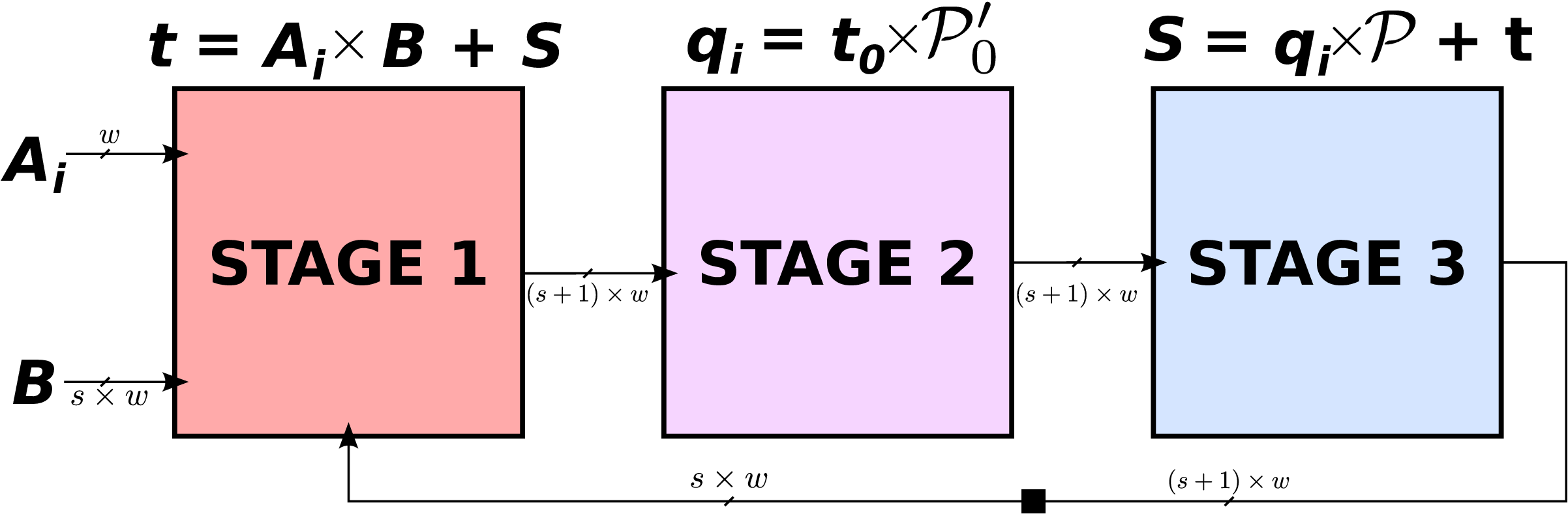
Figure 1: computation stages in the modular multiplication algorithm (from Asilomar 2017 paper).
Proposed Multiplication Units
We propose a new of hardware unit called hyper-threaded modular multiplier (HTMM) to improve efficiency in small hardware units where the modulo p can be selected without constraint at design time. It roughly consists in interleaving independent multiplications in the same hardware resource to fill the pipeline as much as possible. HTMM can be seen as multiple logical multipliers sharing the same physical resource (like in hyperthreaded processors). As illustrated in Figure 2, several couples of operands (A(i) and B(i)) enter successively in the operators. The iterations for the various multiplications are interleaved in the operator. At the end of each internal multiplication (after s iterations), the result product P(i) is available on the output port of the operator.

Figure 2: internal HTMM usage to compute 3 independent MMs (from Asilomar 2017 paper).
The number of “tokens” for independent operations (3 in Figure 2) is determined using algorithms and FPGA parameters to provide very high usage of major internal hardware resources. As the number of parameters is important and they have very different impact of the best type of architecture, we designed a software generator for HTMM. Based on a small set of parameters and optimization directives, it generates synthezisable VHDL descriptions for various HTMM operators and optimizations targets. Figure 3 presents an example of HTMM for 128-bit finite field with a generic p modulo and 3 independent products in parallel for Xilinx FPGAs.
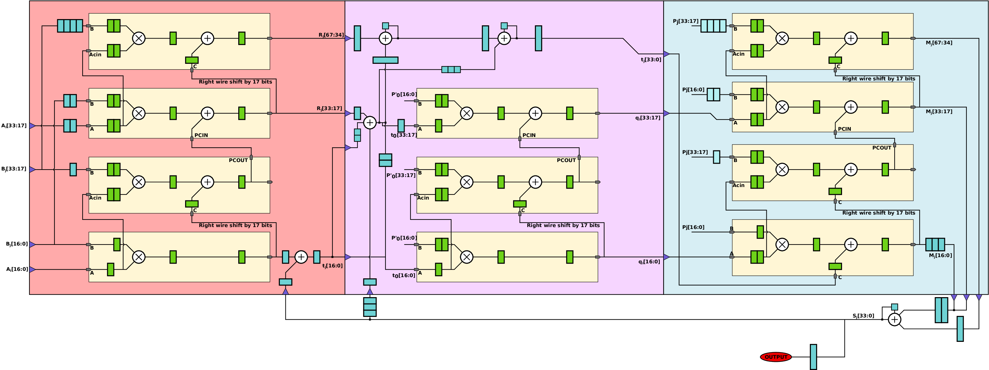
Figure 3: HTMM architecture example for Xilinx FPGAs (from Asilomar 2017 paper).
FPGA Implementation Results and Comparisons
Table 1 reports some results for comparison with the best state of the art multiplier used for ECC (we implemented the multiplier published in article at SAC2013, denoted [6], on the same FPGAs). We implemented 2 HTMM versions on 3 different Xilinx FPGAs: Virtex 5 XC5LX110T (V5), Virtex 4 XC4VLX100 (V4) and Spartan 6 XC6SLX75 (S6). Version HTMM BRAM uses dedicated hardware RAM blocks (BRAMs) to store the 3 pairs of operands. Version HTMM DRAM uses distributed memory in programmable LUTs (lookup tables) of logic slices to store the operands and all intermediate values (no block RAM). All the results are given for providing 3 products (in a hyper-threaded way for HTMM and in a sequential and pipelined way for [6]).

Table 1: Implementation results on various FPGAs for 128-bit MM (from Asilomar 2017 paper).
Main Links:
-
Gabriel Gallin and Arnaud Tisserand: Generation of Finely-Pipelined GF(P ) Multipliers for Flexible Curve based Cryptography on FPGAs. Accepted to the journal IEEE Transactions on Computer, 2019.
- Gabriel Gallin and Arnaud Tisserand: Hyper-Threaded Multiplier for HECC
- Open-source code : https://sourcesup.renater.fr/htmm/
Hardware Accelerators for HECC Scalar Multiplication
We propose hardware accelerators for scalar multiplication HECC based on Kummer surfaces from recent literature. We study and evaluate the impact of various architecture parameters on the cost and performances: type, size and number of units (arithmetic, memory, internal communications); architecture topology; and exploitation of internal parallelism. Several architectures have been designed and implemented on different FPGAs for various parameters, and compared in terms of area and computation time. Our accelerators are designed with internal protections against side channel attacks.
Introduction
A paper presented at CHES 2016 by Rennes et al. (see Links below) proposed a new Kummer-based HECC (KHECC) solution and its implementation on microcontrollers with 30 to 70 % clock cycles count reduction compared to the best similar curve based solutions at equivalent security level. In HAH, we proposed the first hardware architectures for scalar multiplication in KHECC adapted from this paper their FPGA implementations.
KHECC has several advantages:
- smaller finite fields width (half of those for ECC like in typical HECC solutions)
- efficient
xDBLADDoperation for iterations in the scalar multiplication with a constant time and uniform behavior against some side channel attacks - large and regular internal parallelism as illustrated in Figure 1
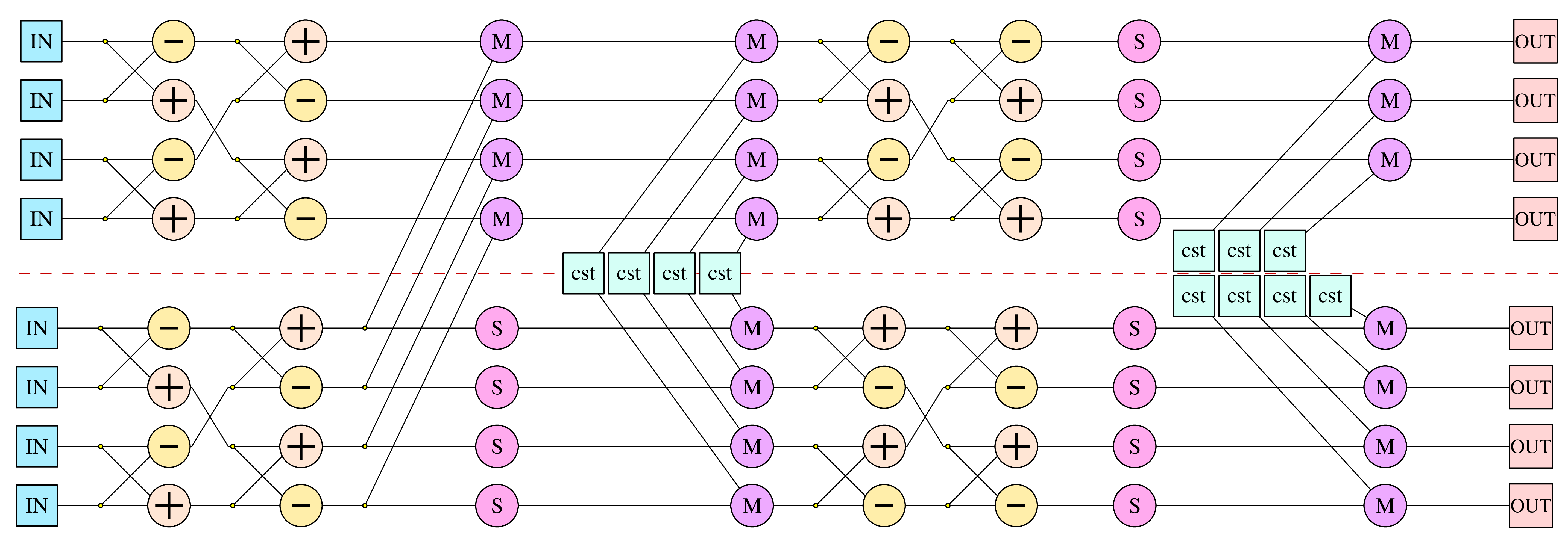
Figure 1: Sequence of finite field operations (Fp) in a xDBLADD operation for scalar multiplication (computation graph obtained from equations in Renes et al. paper).
Objectives
We study and evaluate the impact of various architecture parameters on the cost and performances: type, size and number of units (arithmetic, memory, internal communications); architecture topology; and exploitation of internal parallelism.
We explored several configuration of the internal width (w) of the units and internal communications. The field width is 128 bits with prime p=2127-1.
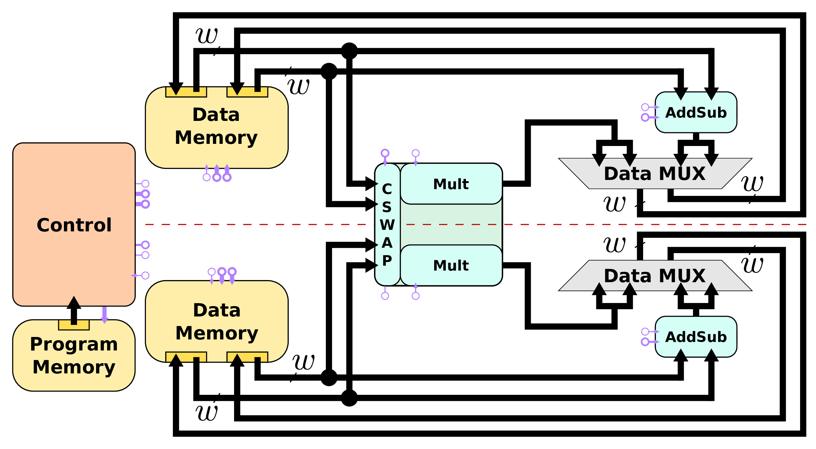
Types of Resources in our Architectures
There are several types of resources in our hardware accelerators:
- arithmetic units for field level operations (F p addition, subtraction and multiplication with generic prime p in this work);
- memory unit(s) for storing intermediate values (F p elements for points coordinates), curve parameters and constants;
- a CSWAP unit in charge of scalar management and on-line schedule of operands depending on scalar/key bit values;
- an internal communication system for data transfers between the units;
- a control based on a microcode running the architecture.
Proposed Architectures
We selected 4 architectures summarized below and fully implemented them in VHDL on several FPGAs:
- Architecture A1: a small and basic embedding the minimum number of units;
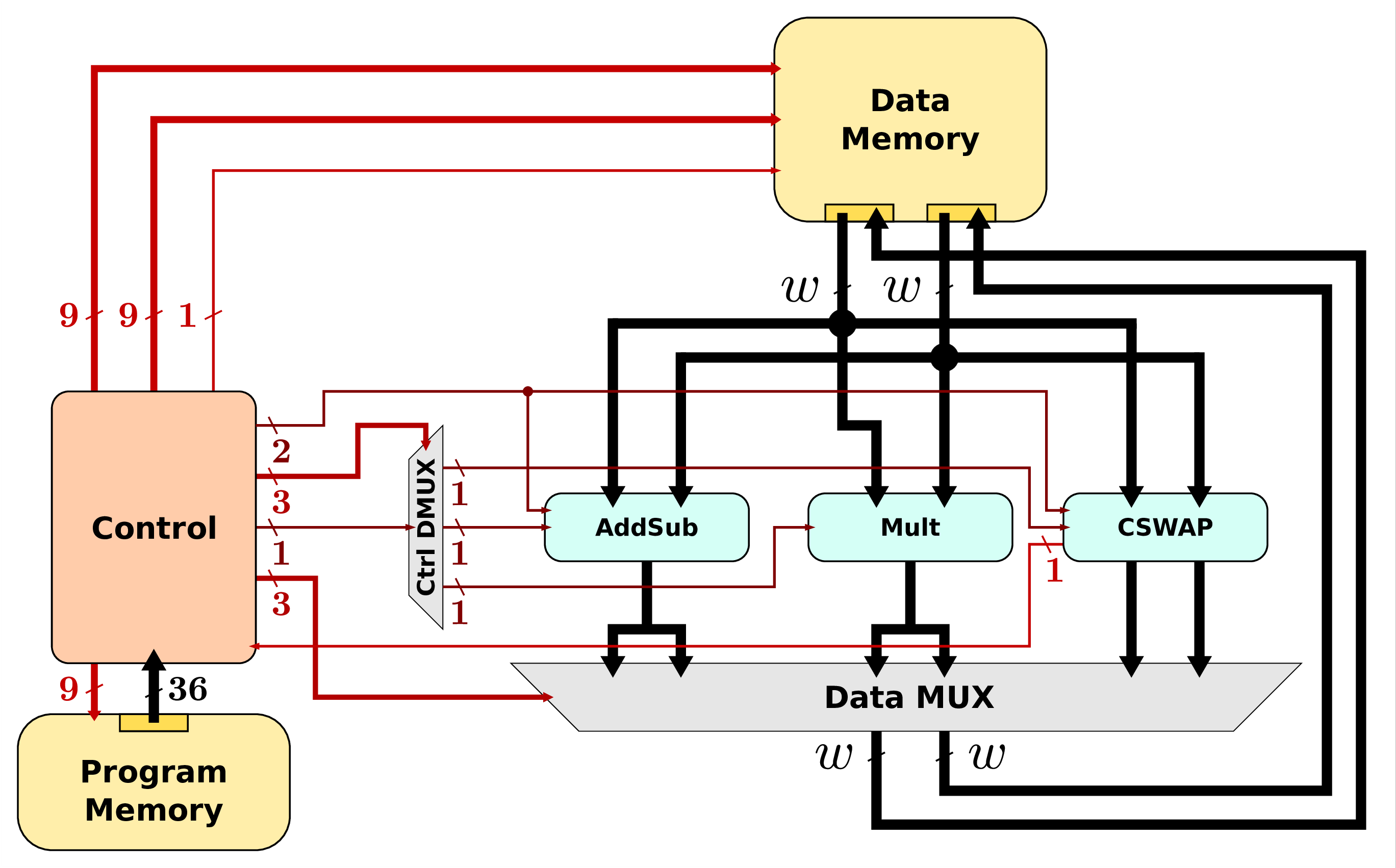
- Architecture A2: A1 with an optimization of CSWAP unit;
- Architecture A3: embeds 2 operators for each arithmetic operation (± and ×) to reach a higher parallelism (notice that a single Mult already handles 3 sets of operands in parallel using hyper-threading, see page on Multipliers);
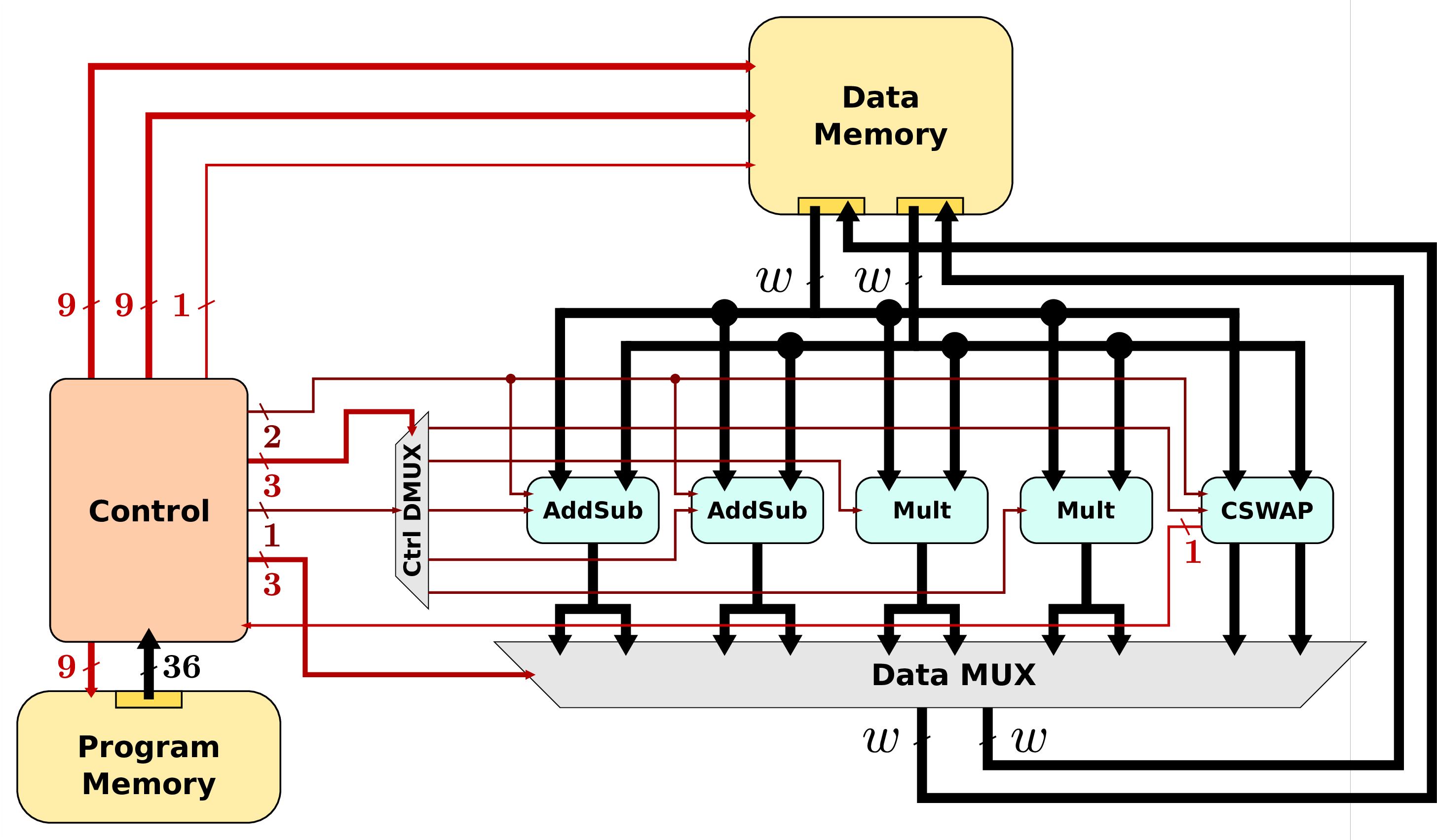
- Architecture A4: a cluster of parallel units for both arithmetic operations and data memory operations, and new version of CSWAP unit.
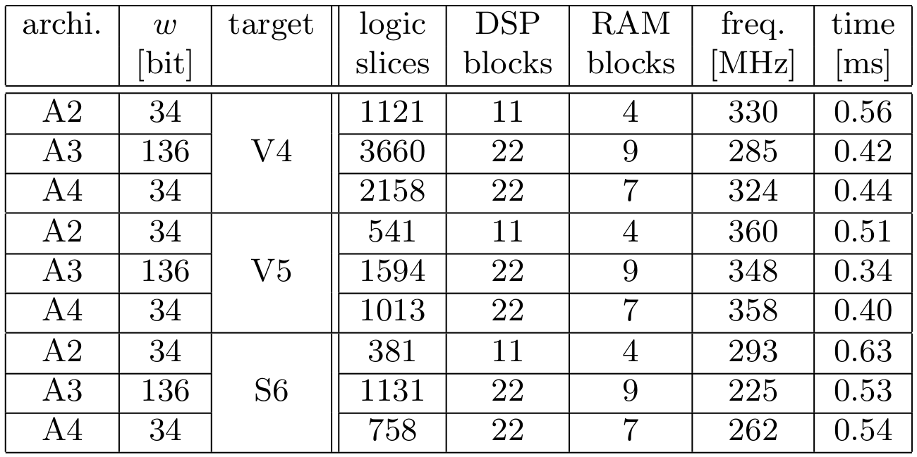
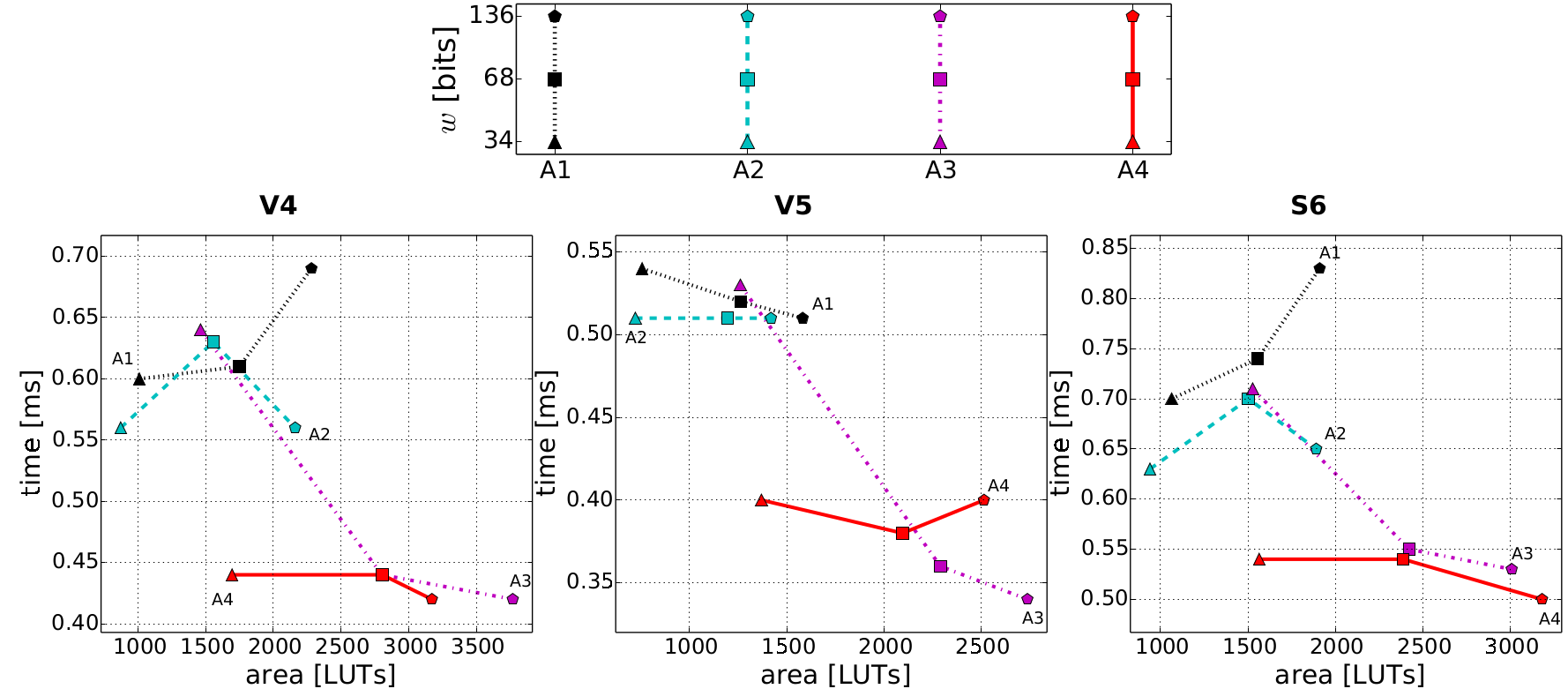
FPGA Implementation Results and Comparisons
All our architectures have been implemented using ISE 14.7 and SmartXplorer (100 runs) tools on 3 FPGAs: Viirtex 4 VLX100, Virtex 5 LX110T and Spartan 6 SLX75.
- Implementation results summary:
- Cost vs performance trade-offs for our architectures:
- Comparisons with ECC solutions from literature (references numbers are in IndoCrypt 2017):
The best configuration depends on theobjective (high speed or low area) and target FPGA. Then exploration toolsat architecture level are helpful for designers and users.
The obtained results lead to similar speed than the best curve based solutions for embedded systems but with an area almost divided by 2 (-40 % for DSP and RAM blocks and -60 % for logic slices).
Main Links:
- Gabriel Gallin and Turku Ozlum Celik and Arnaud Tisserand: Architecture level Optimizations for Kummer based HECC on FPGAs
- J. Renes, P. Schwabe, B. Smith, and L. Batina, “μKummer: Efficient hyperelliptic signatures and key exchange on microcontrollers,” in Proc. Workshop on Cryptographic Hardware and Embedded Systems (CHES), ser. LNCS, vol. 9813. Springer, Aug. 2016, pp. 301–320. DOI: 10.1007/978-3-662-53140-2_15
- Open-source code will be available at the end of the project (due to anonymous submissions constraints)
PhD Theses from the project
- Gabriel GALLIN. Defense scheduled for the 29th of November 2018. Title: Hardware arithmetic units and crypto-processors for cryptography over hyper-elliptic curves. Defense: 29th November 2018, University of Rennes 1. Document and slides acces: TEL-01989822 (PDF).
- . Title: Explicit geometric and arithmetic properties of curves. Defense: 31st August 2018, University of Rennes 1. Document access: TEL-01871465 (PDF).
Award, Invitations and Program Chairs
-
Best paper award for the Architecture track at Compas French conference, June 2015, Lille, France, for the paper (in French) “Comparaison expérimentale d’architectures de crypto-processeurs pour courbes elliptiques et hyper-elliptiques” by Gabriel Gallin, Arnaud Tisserand and Nicolas Veyrat-Charvillon
- Arnaud Tisserand was Program Chair with Julio Villalba of the 22nd IEEE Syposium on Computer Arithmetic (ARITH), June 2015, Lyon, France
- Arnaud Tisserand was Invited Speaker at 19th Workshop on Elliptic Curve Cryptography (ECC), September 2015, Bordeaux, France, on “Hardware Accelerators for ECC and HECC”
- Sylvain Duquesne was Program Chair, with Svetla Petkova-Nikova, of the 6th International Workshop Arithmetic of Finite Fields (WAIFI), July 13-15, 2016 in Ghent, Belgium, Lecture Notes in Computer Science
- Arnaud Tisserand was Invited Speaker at Colloque GDR SOC2, June 2017, Bordeaux, France on “Embedding Crypto in SoCs: Threats and Protections”
- Arnaud Tisserand was Invited Speaker at CRiSIS: 12th International Conference on Risks and Security of Internet and Systems, September 2017, Dinard, France, on “Hardware Support for Physical Security”
- Arnaud Tisserand was the main organizer of CryptArchi 2018: 16th International Wokrshop on Cryptographic Architectures embedded in logic devices, June 2018, Lorient (Guidel-Plages), France.
Futures prospects
We plan to work on more complex architectures for HECC with randomization schemes of the operation flow (for instance commutativity, associativity and distributivity rules can be applied). The internal parallelism in the HECC operation flow may allow us to randomly perform some operations. This should help to frequently change the measured traces during physical attacks (power consumption, timings, electromagnetic emanations). In HAH we used uniform and a constant time algorithm for scalar multiplication (Montgomery Ladder), we plan to compare it with randomized solutions.
In HAH we mainly focused on phyiscal attacks based on observations of side channels. We would like to study protections against fault injection. Then one problem araises. How should be add operations for fault detection in such a way this protection against fault attacks do not increase the vulnerability against observation attacks?