Contents
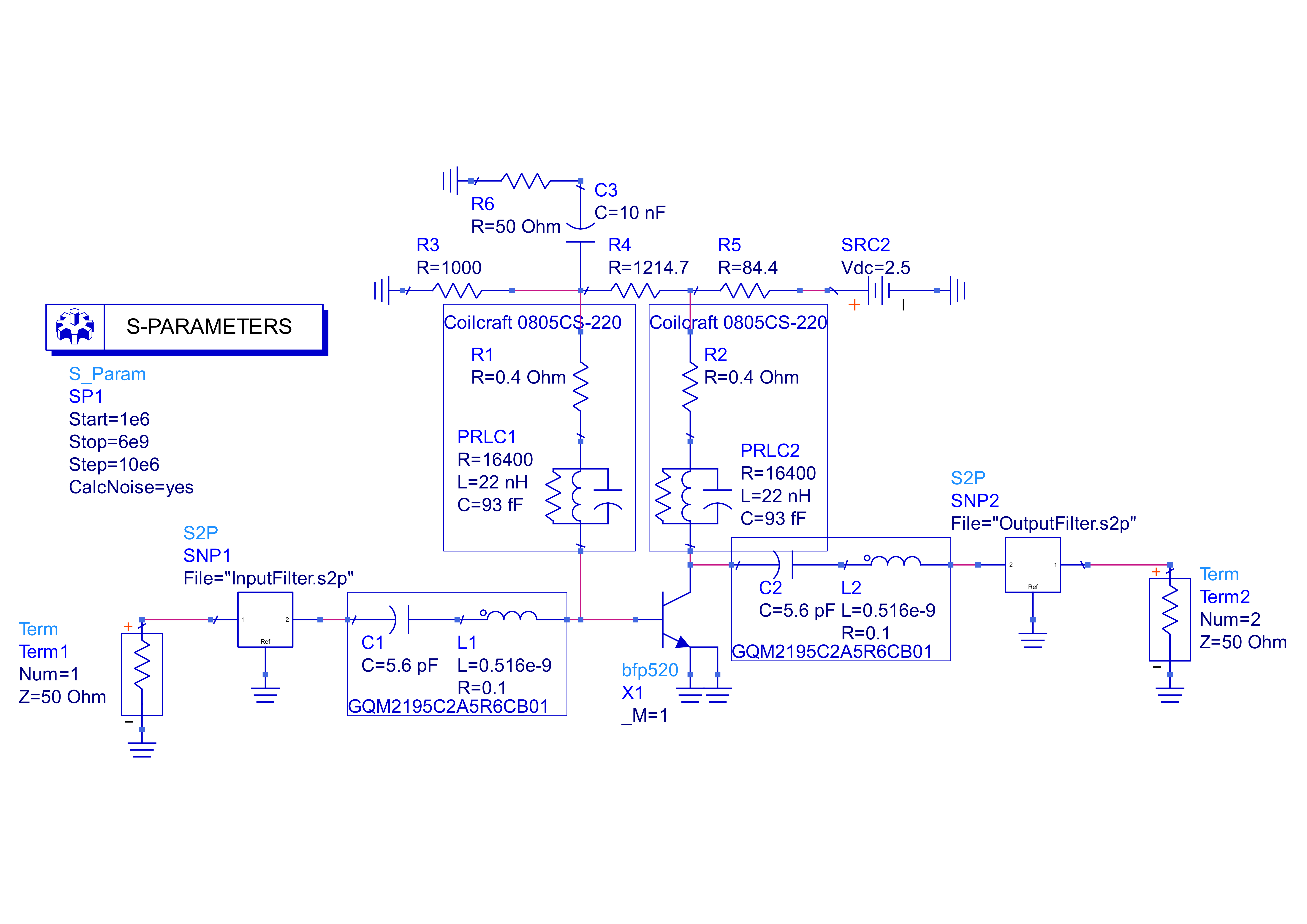
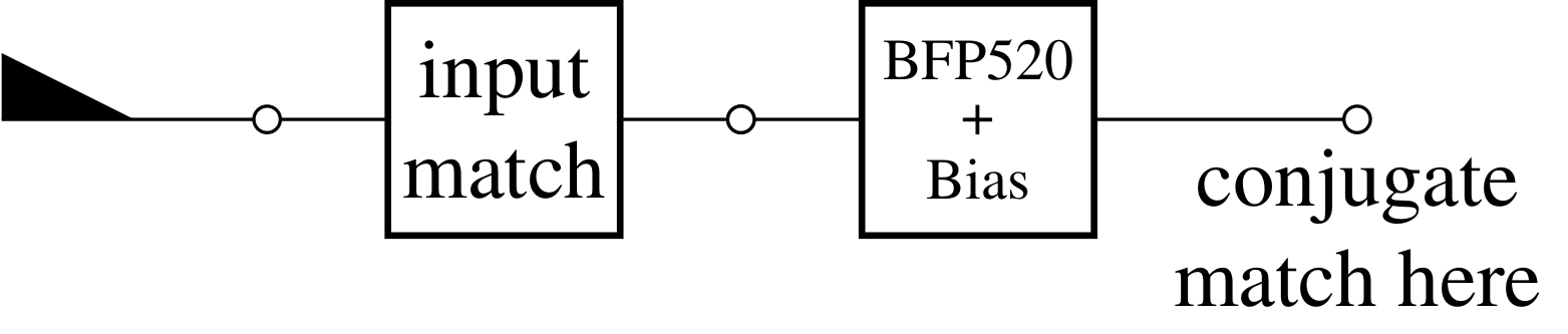
In this script, we design an input and output matching network for a low-noise amplifier based around the transistor infineon BFP520. We can see the ADS schematic of the transistor with the biasing network in the following picture
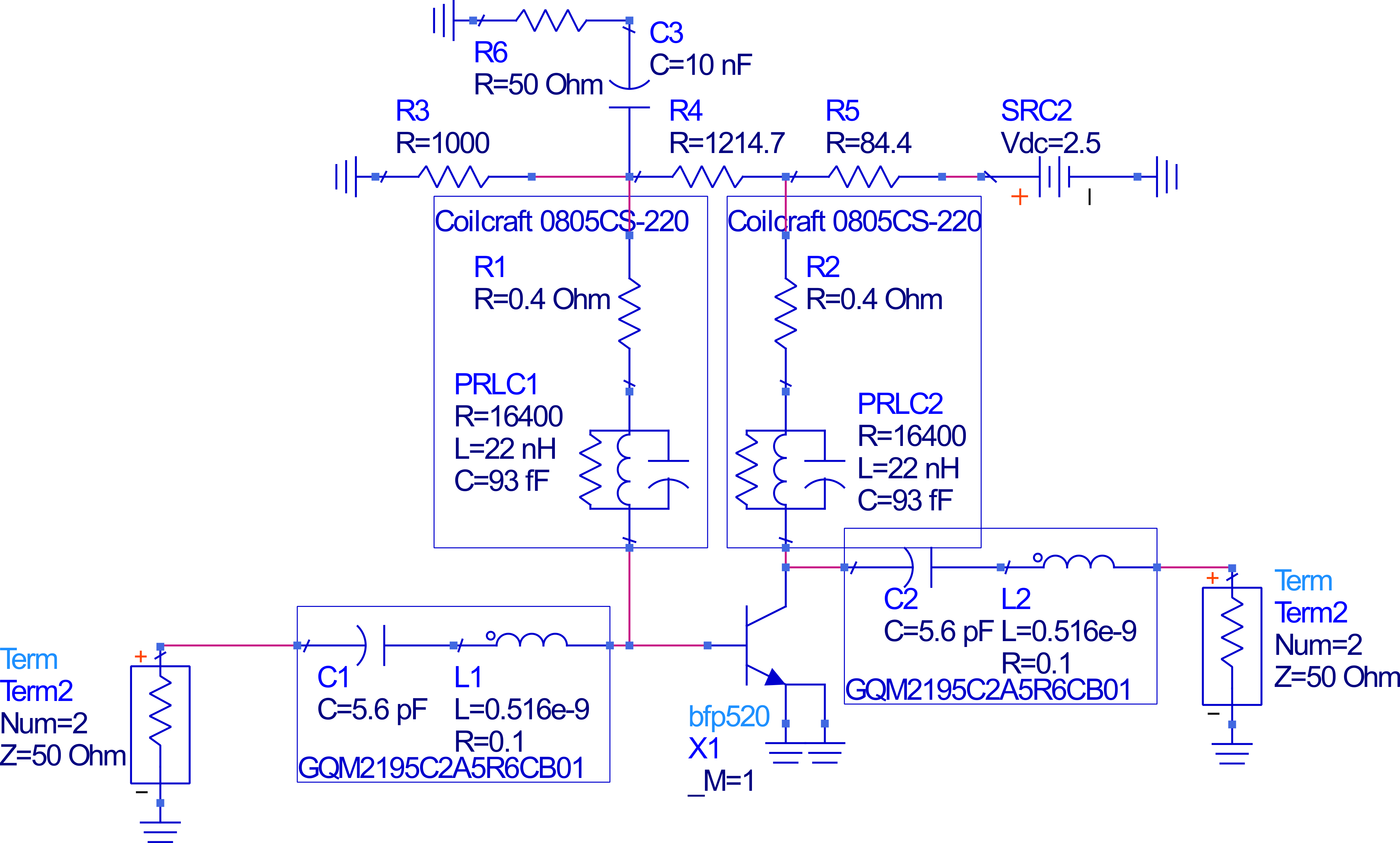
The schematic of the desired system is the following

Loading the simulation data
We simulated the S-parameters and noise parameters of the transistor combined with its biasing network. Those results are stored in the BFP520noise mat file.
We use the function ADSimportSimData from the ADSimportData toolbox to load the data from ADS into the matlab workspace.
1 2 | % Load the simulation data simdata = ADSimportSimData('BFP520noise'); |
with the data imported from ADS we need to construct a MultiPort object containing the reflection \(S_{opt}\) and a TwoPort object with the scattering parameters of the transistor.
3 4 5 6 | % Construct a one-port with Sopt Sopt = MultiPort(reshape(simdata.sim1_S.Sopt,1,1,[]),'Freq',simdata.sim1_S.freq); % Construct a two-port that contains the transistor Tran = TwoPort(simdata.sim1_S.S,'Freq',simdata.sim1_S.freq); |
The frequency band we consider is mainly limited by the design of the biasing network here. With a better inductor, a low noise figure can be obtained over a larger band.
7 8 | % Define the frequency band BAND = FreqBand('Band',[2e9,4e9]); |
Input matching
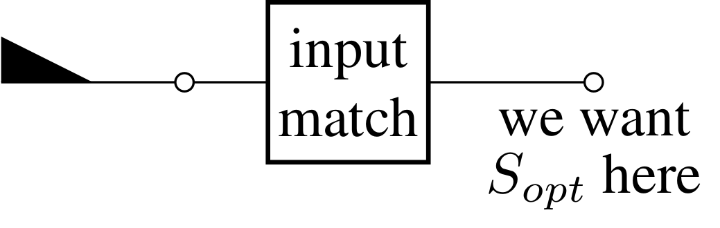
First we design the input matching network, such that the transistor input “sees” Sopt. We do this by synthesising a matching network where conj(Sopt) is the load. The matching network will show at the output the conjugate of the load reflection. Thus we obtain a matching network adapted to \(50\Omega\) at the input and synthesizing \(S_{opt} \) at the output.
We create the input matching object by choosing order 2 for the rational approximation and order 1 for the matching network. Thus we obtain a system of order 3 in this case.
9 10 11 12 13 | % Create matching problem to match to conjugate of Sopt INPUTMATCHING = matching(conj(Sopt),... 'SystemOrder',3,... 'ApproximationOrder',2,... 'Passband',BAND); |
Next the rational approximation of the load is performed
14 15 | % Rational approximation INPUTMATCHING.rationalApproximation; |
The plot function can be used check rational approximation.
16 17 18 19 | % Plot the result of the rational approx figure plot(INPUTMATCHING,'Config','dw') legend('show','Location','Best'); |
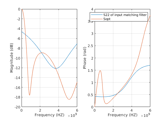
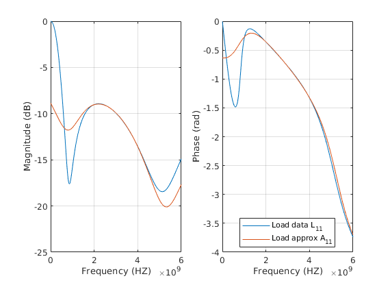 The obtained fit is very good. Then we can solve the matching problem now and plot the results.
20 21 22 | % Solve the matching problemINPUTMATCHING.solve; % Extract the results InputResults = INPUTMATCHING.Results; |
In order to plot the result, the rational model of the matching network need to be evaluated at the frequency points. We can do this with the function getResponse. After that the reflection at the second port of the matching network can be compared with the optimal reflection \(S_{opt} \)
23 24 25 26 27 28 29 30 | % Evaluate the input matching network on the system frequencies InputFilter = InputResults.FILTER.getResponse(Sopt.Freq); % Plot the S22 of the filter and compare to Sopt figure clf, hold on plot(InputFilter.S(2,2,:),'Config','da','DisplayName','S22 of input matching filter'); plot(Sopt,'Config','da','DisplayName','Sopt'); legend('show','Location','Best') |
Output matching
Once we have the input matching network, we compute the S22 of the combination of the input matching and transistor and compute the matching filter for the total network.
To do that we can just cascade the input filter and the transistor with the * operator
31 32 | % Connect the Filter S22 to the input of the transistor
Sys = InputFilter*Tran; |
Note that this design approach will not work every time. It is possible that stability issues are encountered at this stage, but working with an unconditionally stable transistor+biasing will resolve this issue.
Now we create the matching object for the transistor output. We pick again order 2 for the rational approximation and 1 for the matching network (system of order 3).
33 34 35 36 37 | % Create matching problem to match to conjugate of Sopt OUTPUTMATCHING = matching(Sys(2,2,:),... 'SystemOrder',3,... 'ApproximationOrder',2,... 'Passband',BAND); |
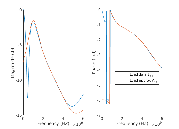
Next we compute the rational approximation of the load seen at the transistor output
38 39 40 41 42 43 | % Rational approximation OUTPUTMATCHING.rationalApproximation; % plot the result of the rational approx figure(54654) plot(OUTPUTMATCHING,'Config','dw') legend('show','Location','Best'); |
Finaly we solve the output matching problem and extract the results
44 45 46 47 48 49 | % Solve the matching problem OUTPUTMATCHING.solve; % Extract the results OutputResults = OUTPUTMATCHING.Results; % Evaluate the output filter on the frequency points OutputFilter = OutputResults.FILTER.getResponse(Sopt.Freq); |
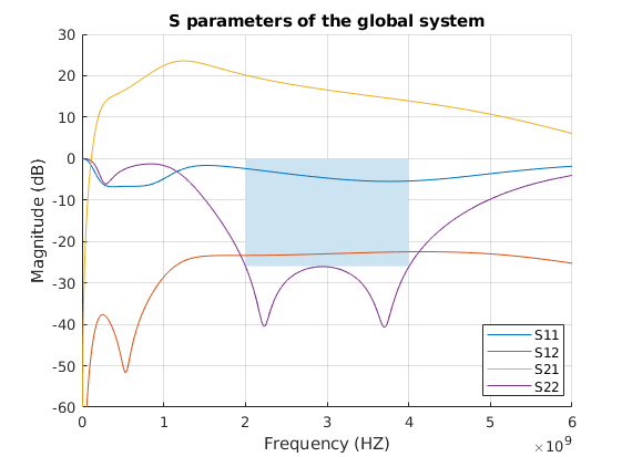
In order to plot the obtained global system we can use again the * operator to cascade all objects and then the plot function. However note that the output matching network is matched to the transistor output at port 2. Therefore this network need to be reverted before cascading.
50 51 52 53 54 55 56 57 58 59 | % Last filter is reverted (matching is performed at port 2 of the filter) TotalSystem = InputFilter*Tran*(OutputFilter(end:-1:1,end:-1:1,:)); % Plot the result figure clf, hold on; plot(OUTPUTMATCHING.Passband); plot(TotalSystem,'DisplayName','S'); ylim([-60,30]); title('S parameters of the global system'); legend('show','Location','Best') |
Finally, we can add both input and output matching networks in the ADS design. We can see next the resulting schematic